Table of Contents
I/O devices
Programming a Z80 CPU is cool, but there are other programmable devices on the Amstrad CPC/Plus motherboard too! These are specialized devices to deal with the video, sound, RAM/ROM mapping, interrupts, … and they can be accessed by the CPU through I/O operations.
It is highly recommended to understand how all these I/O communication things work, especially if you want to bang directly and safely on the bare metal (ie. without relying on the Firmware API). This is going to be a trip in low-level digital electronic realm, but nothing to be afraid of (with a beer or two).
Basic digital electronic knowledge
Lines, buses and direction
Lines
In digital electronics, all devices are connected together with lines. A Line is just a simple wire on the PCB used to transmit a binary information (the signal only takes two values: Low or High), that is, a bit.
Bus
A group of lines is called a Bus. Buses are used to transmit numbers. The more lines, the bigger the number it can transmit (eg. a 8-bits bus consists of 8 lines, therefore it can transmit numbers from 0 (%00000000) to 255 (%11111111)), 2^8 different values.
The two most common buses in computer-system are called the Address Bus and the Data Bus.
Direction
Lines, hence buses too, can be unidirectional or bidirectional.
- When a bus/line is unidirectional, it means that only one single device drives it (ie. sets a value on it) and all the other devices connected to it just read the value (and never, ever, try to write a value on it!).
- With a bidirectional line/bus, several devices can drive the bus to transmit a value but the bus can be driven by one, and only one device at a time. If two or more devices try to drive it at the same time, this may produce a short circuit and blow up some electronic parts! To avoid that, additional control lines are used to indicate the devices what they are allowed to do with the line/bus (ie. to read or write) and, eventually, switch to high impedance state (ie. like if the device was disconnected).
Control Lines
Control lines are mostly output lines from the bus master to the external devices. Only the bus master can assert a level on it's control lines, all the other devices listen to these lines and respond accordingly. These control lines might tell an external device if it should read or write data and when the transfer should happen.
Address bus
Address bus are also output lines that carry information from the bus master to all external devices simultaneously. Again, you can connect these address lines to the input logic of all the external devices simultaneously because only the bus master can write a value on them. Usually, the address lines go to a decoder before going to each device. A decoder is made of one or more chips that recognize when the address lines have been set for the specific device.
In a system with port mapped I/O, an additional control line determines whether the address means access to the memory or an I/O device.
Note that the CPU is not necessarily the only possible bus master:
- On a CPC, the address bus can be driven by the CPU (for memory or I/O read/write operations) or the GA/CTRC (for the display).
- On a Plus, the address bus can be driven by the CPU or the ASIC (display and DMAs)
Data bus and Tri-State logic
 Data lines serve as input and output lines depending on whether the bus master wants to read or to write. The data lines are always connected to each device. As you may know, it is illegal to connect the outputs of logic devices together. If one output wanted to force 1, while the other wanted to force 0, the result would be a lot of power dissipation and a dead chip (bus conflict).
Consequently, all devices that might write to the data bus lines must do so through tri-state logic. As you might guess, tri-state logic has three states:
- High (1)
- Low (0)
- Z (aka high-impedance or High Z state)
If an output is in the High-Z state, it will not draw current from any other outputs to force them into any state. It behaves just as if the gate has been disconnected from the bus.
It may happen that all the devices connected to the data bus are in the High-Z state. In this case, nothing is driving the data-bus to set a value on it, thus all read operation of the data-bus will return an unpredictable value which may vary depending of the electric conditions (weak PSU, additional hardware devices plugged to the Amstrad, …). See the floating bus for more details.
It is the core duty of the bus master to insure that only one device write to the data lines at a time.
Floating bus
 When no device is driving the bus, it's lines are left like disconnected, floating in the air, therefore no real value is fixed on the bus. Usually, no device should try to read the bus in such a state because there's actually nothing to read on it. Nevertheless, if you try do so, for example from BASIC with a
 PRINT INP(&FFFF), a value is returned. So where this value comes from?
In order to register a 0 on a line, current has to be actively sunk out. If the bus is read while all devices are tri-stated, nothing sinks the current, thus &FF is read. But the more stuff is connected to the bus, the more stray capacitance gets added to the lines, the slower the lines will be able to change their state. For example, if the bus contains &00 just before being left un-driven, it will take some time before the stray capacitance rise to 1 again. If the bus is read in the meantime, the voltage won't cross the TTL high level and a zero will be read.
On the Amstrad, there's only once case where you have to deal with this floating bus value, which is when you want to use the Z80 vectorized interrupts mode (See the Z80 IM2 documentation), and that's all.
The floating value on the databus of a bare CPC is usually &FF, but may also even changes periodically (especially, for some unknown reason at the moment, on CPCs fitted with CRTC type 1). On a bare Amstrad Plus, this is usually &78 (no idea why it's not &FF, I bet there's some ASIC mystery involved here).
Any program relying on a floating bus value prediction WILL FAIL. Any programmer doing such crap will be flamed all over the intarweb and fucked in mighty hardware scrollers! I warned you! :)
I/O Mapping
Most I/O devices on the mainboard are assigned to an unique address so that the CPU knows where to find them separately. This unique address is hard wired on the motherboard for each device and it can not (usually) be changed by software. Also, there are two basic approaches to deal with these I/O address:
Memory Mapped I/O (MMIO)
 and I/O devices.") Memory-mapped I/O uses the same address space to address both memory and I/O devices, and the CPU instructions used to access the memory are also used for accessing I/O devices.
Memory-mapped I/O uses the same address space to address both memory and I/O devices, and the CPU instructions used to access the memory are also used for accessing I/O devices.
In order to accommodate the I/O devices, areas of CPU's addressable space must be reserved for I/O rather than memory. The reservation might be temporary (eg. the Amstrad Plus can bank switch between it's ASIC I/O page and regular memory) or permanent.
All I/O devices monitor independently the CPU address bus and respond to any access of device-assigned address space, connecting the data bus to a desirable device's hardware register.
Port Mapped I/O (PMIO)
 and one for I/O devices.") Port-mapped I/O uses a special class of CPU instructions specifically for performing I/O operations. On the Z80 CPU, this is the IN and OUT instructions which can read and write a single byte to an I/O address.
Port-mapped I/O uses a special class of CPU instructions specifically for performing I/O operations. On the Z80 CPU, this is the IN and OUT instructions which can read and write a single byte to an I/O address.
I/O devices have a separate address space from general memory, accomplished by an extra “I/O Request” pin on the CPU's physical interface which indicate if the CPU try to access to the memory or an I/O device.
I/O Decoding
With both memory or port mapped I/O, the I/O address provided by the CPU have to be decoded somehow by the devices. And here again, there are two basic methods to perform this decoding of the I/O address:
Full I/O decoding
|
|
Full I/O decoding involves checking every single line (ie. all bits) of the address bus (and the I/O R/W signal eventually) to determine if a device is selected or not. With Full I/O decoding, each hardware register is mapped to an unique I/O port address. Full address decoding is very efficient in the use of the available I/O address space (one I/O address for one hardware register), but is often impracticable to use because of the excessive hardware needed to implement it. |

Partial I/O decoding
|
|
Partial I/O decoding only checks for a few lines (ie. bits) of the address bus (and the I/O R/W signal eventually) to determine if a device is selected or not. This is the simplest and least expensive form of address decoding and, guess what, this is what is used on the Amstrad of course! :) There are caveats to such simple decoding:
|
.")
I/O devices on the CPC/Plus
Port mapped I/O
|
Memory mapped I/O
|
The port mapped I/O devices on the CPC/Plus use a partial address decoding, hence we got ghost addresses and all the funny stuff :)
The ASIC on the Plus uses memory-mapped I/O to bank switch it's 16Kb I/O page. Moreover, it seems that some “officially unused” addresses in the ASIC I/O page actually produce weird things, so it is more likely that partial address decoding is used within it (but I think no one yet tried to study and document this).
You might have noticed that a device is missing… Where's our beloved soundchip device?! Don't worry, it's fine. The PSG AY3-8912 have no dedicated I/O ports, you have to go through the PPI to access the AY3 (see the PPI documentation).
The Z80 have several control lines, three of them are used for I/O operations:
- IORQ (I/O ReQuest) : Indicate if the CPU is executing an I/O instruction.
- RD (Read) : Indicate if the CPU executes a Read instruction.
- WR (Write) : Indicate if the CPU executes a Write instruction.
Then these 3 signals are mixed to generate two signals actually used by the I/O decoders:
- IORD (I/O Read) : Indicate if the CPU is reading from an I/O address.
- IORW (I/O Write) : Indicate if the CPU is writing to an I/O address.
To simplify all the following I/O illustrations, I used an imaginary IO R/W signal which indicates that the CPU is executing an I/O operation (the I/O ReQuest is active) and is set to R or W (R for IN instructions, W for OUT instructions).
I/O Ports map
| Hardware register | I/O Decoding | Available in | |||||||||||
| Name | R/W | assigned I/O address | Address mask | R/W | 464 | 664 | 6128 | 464+ | 6128+ | GX4000 | DDI-1 | RAM Exp. | |
GateArray | W | &7F00 | 01xxxxxx xxxxxxxx | x | yes | no | no | ||||||
PAL | W | &7F00 | 0xxxxxxx xxxxxxxx | W | no | no | yes | yes1 | yes | yes1 | no | yes2 | |
CRTC Select | W | &BC00 | x0xxxx00 xxxxxxxx | x | yes | no | no | ||||||
CRTC Write | W | &BD00 | x0xxxx01 xxxxxxxx | x | yes | no | no | ||||||
CRTC Status | R | &BE00 | x0xxxx10 xxxxxxxx | x | yes | no | no | ||||||
CRTC Read | R | &BF00 | x0xxxx11 xxxxxxxx | x | yes | no | no | ||||||
Upper ROM | W | &DF00 | xx0xxxxx xxxxxxxx | x | no | yes | yes | yes | yes | yes | yes | no | |
Printer | W | &EF00 | xxx0xxxx xxxxxxxx | x | yes | no | no | no | |||||
PPI PortA | RW3 | &F400 | xxxx0x00 xxxxxxxx | x | yes | no | no | ||||||
PPI PortB | RW3 | &F500 | xxxx0x01 xxxxxxxx | x | yes | no | no | ||||||
PPI PortC | RW3 | &F600 | xxxx0x10 xxxxxxxx | x | yes | no | no | ||||||
PPI Control | W | &F700 | xxxx0x11 xxxxxxxx | x | yes | no | no | ||||||
Soft reset | W | &F8FF | 11111000 11111111 | W | See the note below | ||||||||
FDC Status | R | &FB7E | xxxxx0x1 0xxxxxx0 | x | no | yes | yes | no | yes | no | yes | no | |
FDC Data | RW | &FB7F | xxxxx0x1 0xxxxxx1 | x | no | yes | yes | no | yes | no | yes | no | |
FDC Motor | W | &FA7E | xxxxx0x0 0xxxxxxx | W | no | yes | yes | no | yes | no | yes | no | |
- Hardware Register
- R indicate the register is read only.
- W indicate the register is write-only.
- R/W indicate the register is both readable and writable.
- I/O Decoding
xindicate a bit ignored by the I/O decoding.0indicate the bit must be clear to select the device.1indicate the bit must be set to select the device.Windicate the device will respond only to an I/O Write operation.
- Note 1: The 464Plus and GX-4000 are cut-down versions of the 6128Plus. All these models are based on the same ASIC chip which emulate some devices from the classic CPC (ie. Gate Array, PAL, CRTC and PPI). Therefore the PAL is emulated by the ASIC of the 464Plus and GX-4000 but the PCB is missing some electronic parts so it is not working (and you should not use it in this case).
- Note 2: A PAL (compatible with the one in the 6128) is available in some (but not all!) RAM Expansion devices (eg. Dk Tronics RAM Expansion).
- Note 3: Each port of the PPI can be configured, through the PPI control port, as Input or Ouput (or even in some case, bidirectional).
This is only the I/O port map of standard Amstrad I/O devices! There's many others third-party devices available with well known (hence reserved) I/O port addresses. An exhaustive I/O port summary is available on CPC-Wiki.
Soft Reset
The Firmware MC BOOT PROGRAM and MC START PROGRAM functions both write 255 to I/O port &F8FF when they are executed (eg. after RUN”FOO in BASIC). This is probably intended to allow peripherals to reset themselves, if needed, when a program is started.
This is an undocumented feature and no peripherals are known to take advantage of it. Such peripheral should, as much as possible, perform a complete decoding of the I/O address on a Write access only to avoid unintended peripheral-reset with program messing with ghost I/O addresses.
KISS principle
In reality, most I/O devices on the Amstrad check only for one bit of the address bus (when the IORQ control line from the CPU is active) and sometime the RW control line too. But many devices provide several hardware registers (eg. CRTC, PPI, FDC) which are selected according to fews other bits of the address bus and are not, electronically speaking, part of the I/O decoding process.
For sake of simplicity, I considered those bits, used to select one of the hardware registers of a device, part of the I/O decoding process. From a programming point of view, it won't change anything. If you're getting confused, get a beer, now!
(See KISS principle definition too :)
CPU I/O Instruction set
IN (I/O Read)
|
OUT (I/O Write)
| ||||||||||||||||||||||||||||||||||||||||||||||||||||||||||||||||||||||||
For Symbolic Operation:
- (HL)
- Memory access at the address pointed by HL.
- [BC] or [An]
- Read from (IN) or Write to (OUT) the I/O Address pointed by BC or An.
Amstrad fantasy
The Z80 was officially described as supporting 8 bit (256 ports) I/O-addressing. It's I/O instruction set is designed to address the I/O device with the lower half of the address bus (A7-A0). However, it can be seen that all I/O instructions actually assert the entire 16-bit address bus (A15 to A0) and not only the lower-half (A7 to A0).
A designer could choose to decode the entire 16 bit address bus on I/O operations in order to take advantage of this feature, or just stick to the Zilog's guidelines and decode only the lower half to select an I/O device (and eventually use the upper half to select sub-features of the I/O device).
Amstrad has chosen to decode the upper half (A15-A8) of the address bus to select a device instead of the lower half (A7-A0)!
It severely affects the CPU I/O instruction set:
OTIR, INIR, OTDRandINDRare unusable.OUTI, INI, OUTDandINDrequire some walk-around to be used.OUT (n),AandIN (n),Aare barely usable.- (And the instruction syntax with
(C)doesn't make sense any more, it should be noted(B)on the Amstrad! :)
Special devices
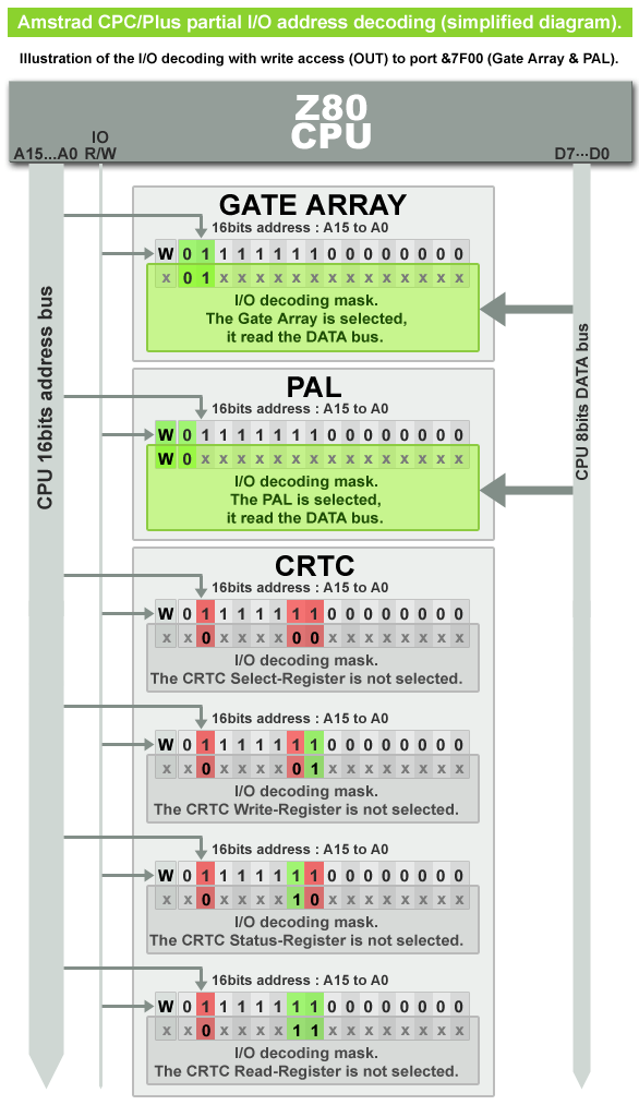
&7F00: Gate Array and PAL
|
|
These two devices might need some enlightenment. As seen from the I/O port map, they are both located at the same I/O address: &7F00, so they are both active when the CPU write a value to that address! Alert! Alert! Bus conflict incoming! Alert! Well, relax! Everything is under control! :) The Gate Array and PAL are designed to work safely together at the same I/O address without any problems (The PAL is designed to expand the command set of the Gate Array). Electrically, there's no problem because they are both write-only device, they can not drive the DATA bus, they can only read it's value. When an I/O request is issued at their I/O address, how do they know which one of them have to handle it? It's done by analyzing the value on the DATA bus (which is usually sent by the CPU, otherwise… ermm :). If it's an MMR command, the PAL will process it. If it's a GA command (INKR, PENR, RMR), the GA will process it. It is not possible to send a valid command code on both the GA and PAL at the same time and if the value on the DATA bus does not match any valid command code, the I/O request will be simply ignored (and nothing happens). You will find more detailed informations in the Gate Array and PAL documentation. |
&DF00: Upper ROM Register
(todo)
Programming I/O devices
It is not recommended to bang directly on the hardware when the Amstrad firmware is up and running. You have to use the firmware API if you wanna do something with the hardware, so that the firmware will know and keep track of it. It's very important especially for ROM mapping with the RMR register of the GateArray and the Upper ROM Register!
Conventionnal I/O programming
Conventionnal I/O programming means that you only use the allocated standard I/O ports (which were chosen to avoid bus conflict between devices). That's the safest way to go most, if not all, the time.
The standard I/O port addresses are 16bits, however the devices I/O decoding in the CPC use mostly the upper half (A15 to A8) of the address (except the FDC which decodes address bits in the lower half too, see the I/O port map). So you can choose to use the full 16bit address or just the upper half of it.
Full 16bits; Set BC with the full 16bits ; I/O address of the CRTC Select register ld bc,&BC00 ; Load the value to write to the CRTC ld a,12 ; Select CRTC Register 12 out (c),a Safe, yeah, but a little bit bulky doesn't it? Unless you're dealing with the FDC, you should use the Upper-half 8bit version instead. |
Upper half 8bits; Set B with only the upper half of the ; I/O address of the CRTC select register ; Set C with the 8bits value ld bc,&BC00+12 ; Write 12 to port address &BCxx out (c),c It does exactly the same thing than the full 16bits example, but using only the upper half of the I/O address. It will save some CPU cycles and RAM space, and you can do that for all I/O device (but the FDC). |
Guru I/O programming
(todo)
Jackass I/O programming
- The stunts illustrated here were performed by trained professionals! DON'T DO THAT AT HOME KIDS!
- I decline all responsibility for any damages that may result from using this website and the information contained herein.
- You assume full responsibility for direct or indirect losses, smokes, screams, explosions, fire or damage of any nature and extent that may derive from the use of this site.
- Short version: Don't blame ME if YOU blow up your Amstrad :).
These are just two bus conflict examples. Basically, it can happen with any I/O device which can write something to the data bus.
You must be extremely cautious when dealing with ghost addresses, because it's very likely that more than one I/O device might respond at the same time. It's not always a problem but as soon as there is a problem, it's not just that your program won't work, it's that it may blow up your Amstrad! (I experimented nasty things on the Amstrad CPC and never blowed up anything yet, but you've been warned! :).
Write to a Read Only hardware register
") The CRTC 6845 has two read only registers located at &BE00 and &BF00 I/O addresses. As soon as it decodes an I/O access to one of these registers, it will drive the databus to set a value on it, no matter what the I/O direction is (Read or Write). If the CPU intends to write to these registers, then there's a problem because both the CPU and the CRTC will try to drive the data-bus at the same time.
The CRTC 6845 has two read only registers located at &BE00 and &BF00 I/O addresses. As soon as it decodes an I/O access to one of these registers, it will drive the databus to set a value on it, no matter what the I/O direction is (Read or Write). If the CPU intends to write to these registers, then there's a problem because both the CPU and the CRTC will try to drive the data-bus at the same time.
ld bc,&BF00 ; CRTC Read register I/O address
out (c),c   ; Write 0 at this address
Of course, seen like this, it looks pretty stupid to do that (Yes! It does! :). But as soon as you deal with ghost addresses for some hardcore optimization, it won't be so obvious.
This case may happen with any device with read-only register(s) (eg. FDC).
Illegal/Ghost I/O address
 using OUTI/OUTD instruction! Be carefull!")
ld bc,&BB00 ; Illegal I/O address
out (c),c   ; Write 0 at this address
Is the same than:
ld hl,pointer_to_some_crtc_data
ld bc,&BC00
outi
&BC00 is the standard CRTC Select register I/O address, but the OUTI/OUTD instructions pre-decrement register B before performing the I/O operation, so the I/O will hit port &BB00 instead of &BC00! Fail!
All hail to High impedance!
Blind test
I've heard of a common I/O misundestanding on the Amstrad, which is about the high impedance state of I/O devices. The most infamous example is that:
	; Detect CPC or Plus machines
	ld bc,&7F00		; Gate Array/PAL I/O address
	in a,(c)		; Read?! a Write-Only I/O port?!?
	cp &FF			; &FF.. w00t?
	jr z,CPC_detected	; Maaagic!
	; Plus detected
This little code snippet has been used to detect the Plus machines in several productions (and failed on my Plus on several occasions). But let's see what it really does.
Obviously, we are dealing with the Gate Array and PAL I/O port:
ld bc,&7F00
Then an I/O read operation is issued:
in a,(c)
Which is quite stupid since the Gate Array and PAL are both Write-Only devices (from the CPU point of view). They can not write anything to the DATA bus! So what's happening then?
- The PAL (if available) is disabled because it checks the I/O direction and works only with I/O Write operation.
- The Gate Array is enabled (it doesn't care about the I/O direction at all).
- Both the CPU and the Gate Array expect to read something on the DATA bus, therefore the DATA bus is left in high impedance state (nothing is driving it).
- The CPU and the Gate Array read the value on the DATA bus in high impedance. This value is absolutly not predictable and may vary.
- If this value correspond to a valid Gate Array command code (RMR, INKR, PENR), it will be issued (if it's an RMR code, it will page in/out ROMs and most probably crash your program!).
Then, on the CPU side, the value is compared to &FF:
	cp &FF
	jr z,CPC_detected
Why &FF? On a healthy and bare Amstrad CPC, that's the value you can usually read on the DATA bus in high impedance state. On a healthy and bare Amstrad Plus, this is usually &78.
So it seems to work fine! Yep, but at some point, it will also fail! When the machine is aging or you start pluging expansion boards or new cartdridge (on a Plus), this will affect the unstability of the DATA bus in high impedance state. Moreover, what the fuck is the Gate Array doing here? There's no need of it unless you want to crash your program randomly!
There's much more reliable methods to detect a Plus machine, only idiots still use this awful “trick”.
Random Jumps
An other example of how to fuck up your wonderful program with the high impedance state is with the vectorized interrupt mode (IM 2).
(todo)
When the DATA bus is in High Impedance state, it's value is unstable and may vary from one machine to another, depending mostly on what and how many expansion boards are connected, the overall health of the machine (mainboard and PSU), atmospheric pressure, direction of the wind and temperature of your beer…
You should never do anything relying on the value of the DATA bus in High impedance state and expect it to work the same on all machine. It won't!
You should never do anything relying on the value of the DATA bus in High impedance state and expect it to work the same on all machine. It won't!
I/O Simulator
(todo)