The Gate Array
A Gate Array (aka ULA) is a custom chip that can be designed to accomplish specific functions in a single chip, thus reducing manufacturing cost alot (smaller PCB, less electronic parts needed, lower power requirements, …).
On the Amstrad CPC, the Gate Array is clocked at 16MHz and designed for:
- Producing all the clocks signals (1MHz and 4MHz).
- Generating a CPU maskable interrupt.
- Handling Lower and Upper ROMs signals.
- Video mode and palette.
- Converting RAM data into RGB signals.
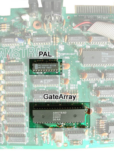
Hidden behind the famous Gate Array, there's an other custom chip on 128k machines, a Programmable Array Logic, to extend the functionnalities of the Gate Array and manage the extended RAM.
All the Amstrad CPC 6128 have it built-in to handle the internal 64Kb RAM expansion. The 64Kb CPC (ie. CPC464 and CPC664) don't have it, but a 6128 compatible PAL can be provided by an external RAM expansion device connected to the machine. Some RAM expansion manufacturers, e.g. Dk'Tronic, embed a 6128-compatible PAL within the interface, however some manufacturers also used their own proprietery RAM management system (incompatible with the 6128 PAL).
External links
Further informations about the Gate Array & PAL can be found on these websites:
|
|
Versions history
Different versions of the Gate Array exist. They basically all do the same things, but their technology and design have been improved in the latest revisions.
Amstrad 40007 (CPC 464)
The first version of the Gate Array is the 40007 and was released with the CPC 464. Some of them are mounted with a huge and ugly heat sink.
Amstrad 40008 (CPC 664)
Later, the CPC 664 came out fitted with the 40008 version (and at the same time, the CPC 464 was also upgraded with this version). This version is pinout incompatible with the 40007 (that's why the upgraded 464 of this period have two Gate Array slots on the motherboard, one for a 40007 and one for a 40008).
Amstrad 40010 (CPC 6128)
The CPC 6128 was released with the 40010 version (and the CPC 464 and 664 manufactured at that time were also upgraded to this version). The 40010 is pinout compatible with the previous 40008.
Amstrad 40226 (Costdown CPC)
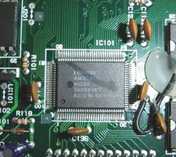 In the last serie of CPC 464 and 6128 produced by Amstrad in 1988, a small ASIC chip have been used to reduce the manufacturing costs. This ASIC emulates the Gate Array, the PAL and the CRTC 6845. And no, there is no extra features like on the Amstrad Plus. The only noticeable difference seems to be about the RGB output levels which are not exactly the same than those produced with a real Gate Array (I'm looking for a costdown CPC to measure this exactly and see if it's true, or not. If you have one to spare or lent me, get in touch).
The Gate Array and PAL are no longer distinct onboard chips but they are emulated by this ASIC.
Amstrad 40489 (Plus & GX-4000)
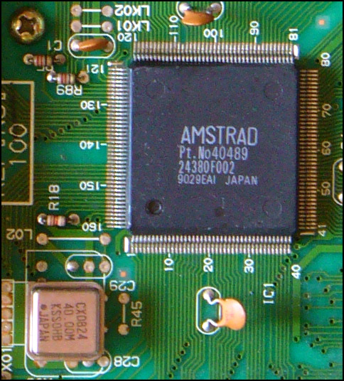 All the Plus range is built upon a bigger ASIC chip which is integrating many features of the classic CPC (FDC, CRTC, PPI, Gate Array/PAL) and all the new Plus specific features. The Gate Array on the Plus have a new register, named RMR2, to expand the ROM mapping functionnalities of the machine. This register requires to be unlocked first to be available. And finally, the RGB levels produced by the ASIC on the Plus are noticeably differents (not that much, but enough to piss off many CPC artists :).
The Gate Array and PAL are no longer distinct onboard chips but they are emulated by this ASIC.
Description
The Gate Array is a multifunctions chip. It handle the ROM mapping, the interrupt generator, and video. When a PAL is available (CPC 6128 or any CPC with a RAM expansion), it also manage the RAM mapping to access to the extended memory.
ROM/RAM mapping
Interrupt generator
Amstrad CPC
The CPU maskable interrupts are generated by the Gate Array. This is done by using a 6bits internal counter and monitoring the HSync and VSync signals produced by the CRTC.
On every falling edge of the HSync signal, the Gate Array will increment the counter by one. When the counter reaches 52, the Gate Array raise the INT signal and reset the counter. With 50Hz PAL CRTC settings (one HSync every 64us) this will produce a 300Hz interrupt rate.
When the CPU acknowledge the interrupt (eg. it is going to jump to the interrupt vector), the Gate Array will reset bit5 of the counter, so the next interrupt can't occur closer than 32 HSync.
When a VSync occurs, the Gate Array will wait for two HSync and:
- If the counter>=32 (bit5=1), then no interrupt request is issued and counter is reset to 0.
- If the counter<32 (bit5=0), then an interrupt request is issued and counter is reset to 0.
This 2 HSync delay after a VSync is used to let the main program, executed by the CPU, enough time to sense the VSync (for synchronisation with the display, most likely) before an interrupt service routine is eventually executed.
So all the interrupt timings are mostly determined by the CRTC settings. Other than that, the internal interrupt counter can be cleared anytime by software using the Gate Array RMR register.
Timings
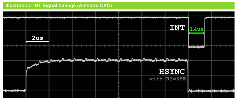
The INT signal (active low) produced by the Gate Array, is a short pulse of 1.4us and starts right after the falling edge of the HSync signal (produced by the CRTC).
Amstrad Plus
Unlike the CPC, the Plus have several interrupt sources:
- Raster Interrupt
- DMA0
- DMA1
- DMA2
The raster Interrupt can be programmed to behave like the CPC interrupt (every 52 HSync) or to be issued at a specific HSync in the video frame. The 3 DMA channels can also be programmed to trigger an interrupt. You will find more informations about the ASIC interruptions in the ASIC documentation.
One important thing is that the ASIC trigger the interrupt about 1us later than the CPC, therefore all CPC programs synchronizing video effects (raster most likely) with a HALT instruction will be 1us late on the Plus. You can adjust that with the CRTC register 3.
Video
RGB Outputs
Composite Sync
I/O Decoding
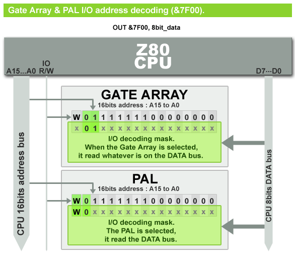 The Gate Array and PAL are two differents chips but they respond to the same I/O port (&7F00). When an I/O request is sent to this port, they will both examine the 8bits data to determine what command it is. If they recognize a valid command code, they will execute it otherwise they will ignore it. Both chips have distinct command codes, it is not possible to affect these two chips at the same time with a single command code, it's a Gate Array only command code or a PAL only command code.
I know that some people are doing just that, reading I/O &7F00, to detect a Plus machine. Well, it seems to work because the high-impedance state is not the same between a CPC and Plus (without going into deep detail, it's related to impedance/capacitors and others stuffs which all vary greatly with time, heat, etc). This is absolutly not reliable! Don't do such crap and forget about it! Thanx :)
Registers
The GA features differents registers controlling various things in the CPC/Plus, such as video mode, colors, ROM and RAM memory mapping, 300Hz interrupt counter. These registers are selected with bit7 to 5 of the 8bit command-code written at the I/O address &7F00 where the GA/PAL are located. Bits 4 to 0 hold the command paramater.
| 8bit command | |||||||||||
|---|---|---|---|---|---|---|---|---|---|---|---|
| 7 | 6 | 5 | 4 | 3 | 2 | 1 | 0 | Machine | Register | Description | Chip |
| 0 | 0 | 0 | n | All | PENR | Select a color register | Gate Array | ||||
| 0 | 0 | 1 | n | All | PENR | Ghost register | Gate Array | ||||
| 0 | 1 | 0 | n | All | INKR | Change the value of the currently selected color register | Gate Array | ||||
| 0 | 1 | 1 | n | All | INKR | Ghost register | Gate Array | ||||
| 1 | 0 | 0 | n | All | RMR | Control Interrupt counter, ROM mapping and video mode | Gate Array | ||||
| 1 | 0 | 1 | n | All | RMR | Ghost | Gate Array (CPC) or locked ASIC (Plus) |
||||
| 1 | 0 | 1 | n | Plus | RMR2 | ASIC & Advanced ROM mapping | Unlocked ASIC | ||||
| 1 | 1 | n | All | MMR | Memory mapping | PAL | |||||
Bit5 and compatibility between CPC and Plus
On a real Gate Array (CPC 464,664 and 6128), bit5 of the command have absolutly no effect and can be set to 0 or 1. However, on a Plus machine with it's RMR2 register unlocked, this bit is used to select the RMR2 register.
PENR
This register can be used to select one of the 17 color-registers (pen 0 to 15 or the border). It will remain selected until another PENR command is executed.
| PENR | Index | |||||||
|---|---|---|---|---|---|---|---|---|
| 7 | 6 | 5 | 4 | 3 | 2 | 1 | 0 | color register selected |
| 0 | 0 | 0 | 0 | n | pen n from 0 to 15 | |||
| 0 | 0 | 0 | 1 | x | x | x | x | border |
- x can be 0 or 1, it doesn't matter.
Exemple
; select pen 5
ld bc,&7F05
out (c),c
; all INKR command will affect pen 5 until a new PENR command
; is executed to select another color-register.
INKR
This register takes a 5bits parameter which is a color-code. This color-code range from 0 to 31 but there's only 27 differents colors (because the Gate Array use a 3-states logic on the R,G and B signals, thus 3x3x3=27).
| INKR | Color | |||||||
|---|---|---|---|---|---|---|---|---|
| 7 | 6 | 5 | 4 | 3 | 2 | 1 | 0 | |
| 0 | 1 | 0 | n | where n is a color code | ||||
The PEN affected by the INKR command is updated (almost) immediatly (does someone said… raster bars? :).
Exemples
; Select the border with a PENR command
ld bc,&7F10
out (c),c

; Set the currently selected color register to black with an INKR command.
ld bc,&7F54 ; &54 = INKR code for black (see colors table)
out (c),c
INKR color-codes
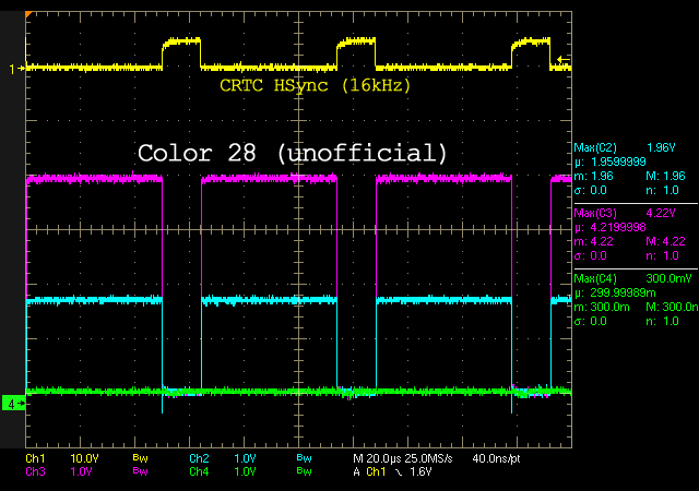
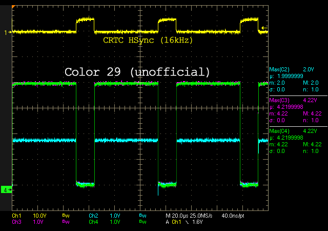
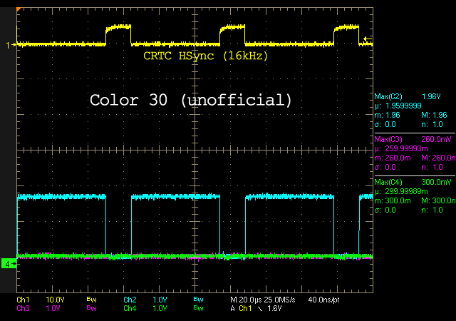
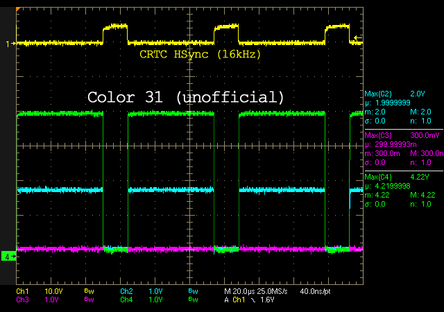
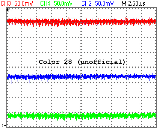
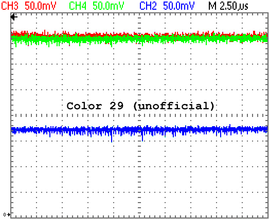
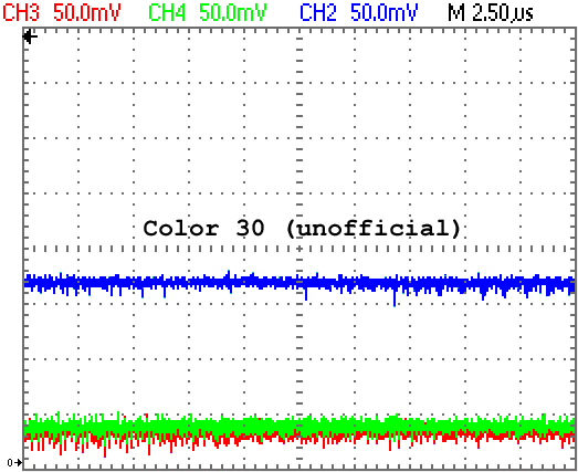
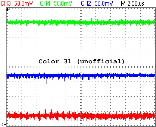
The table below shows the 32 possible colors with the Gate Array, sorted on their luminosity (on a green screen), from dark (0) to bright (26). The colors 27 to 31 are ghosts from officials colors with very slight changes on the R,G and B levels.
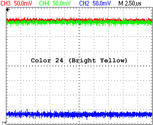
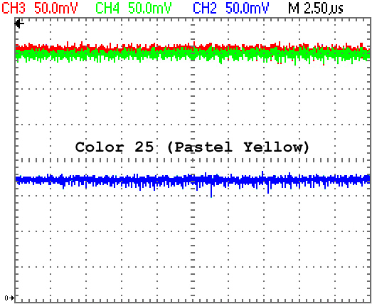
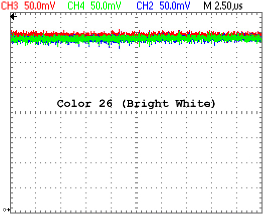
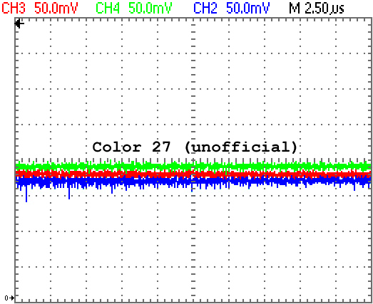
The colors codes are indicated for BASIC (aka software color code), Gate Array (the INKR command, aka hardware color code) and 12bits GRB value produced by the ASIC when it translate an INKR command.
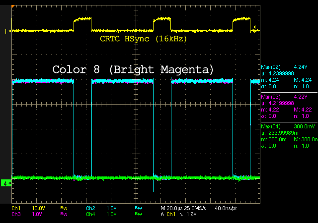
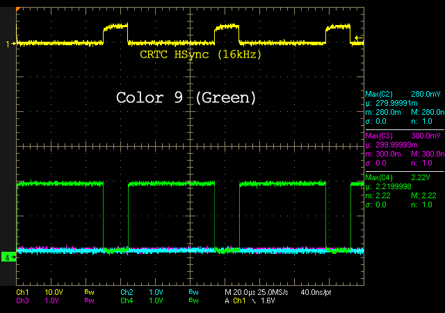
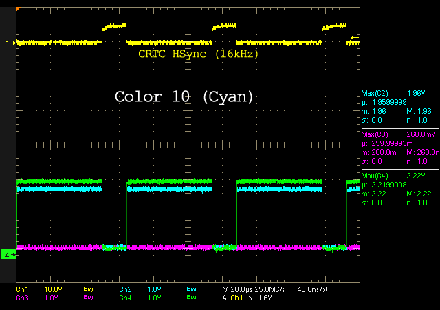
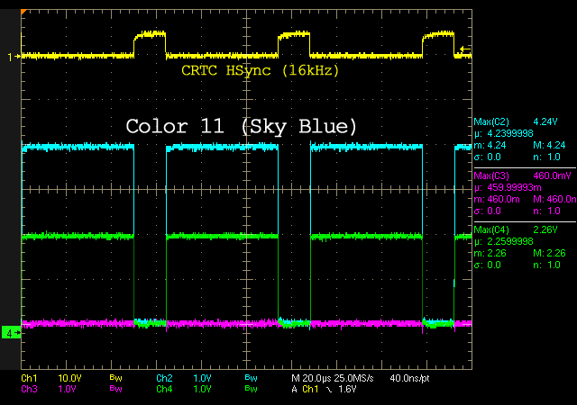
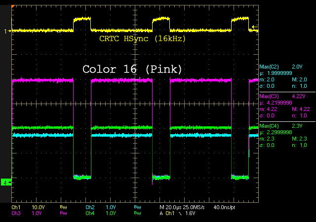
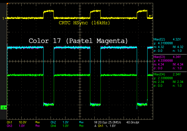
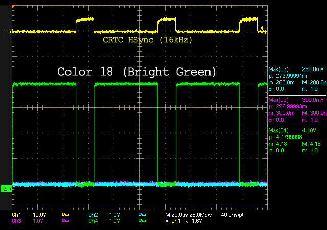
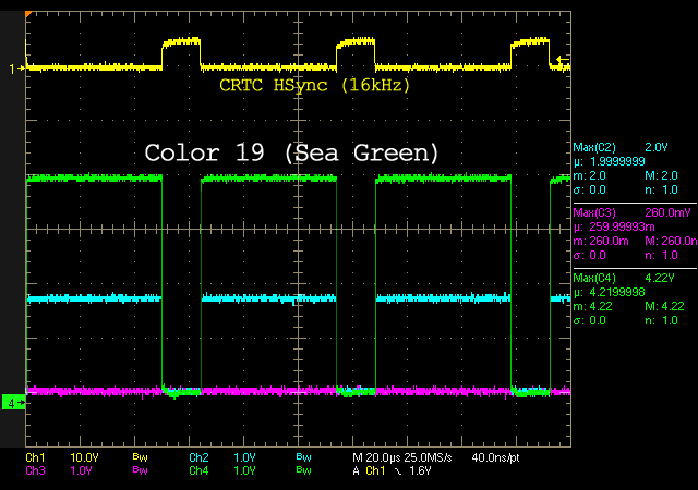
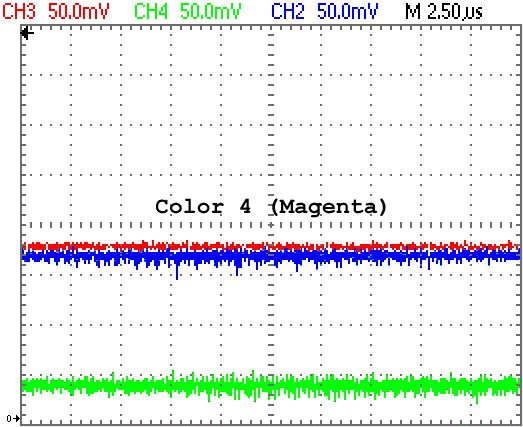
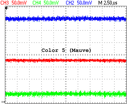
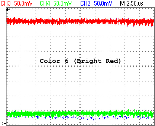
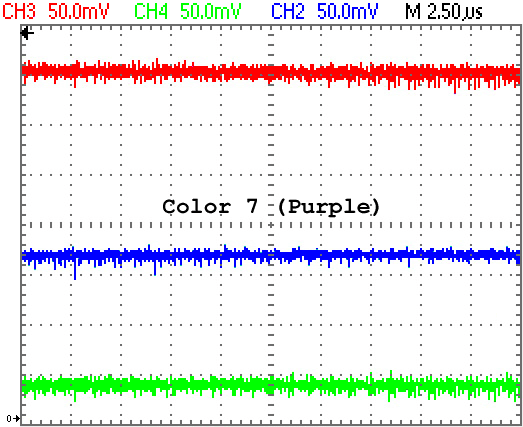
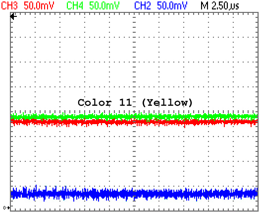
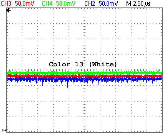
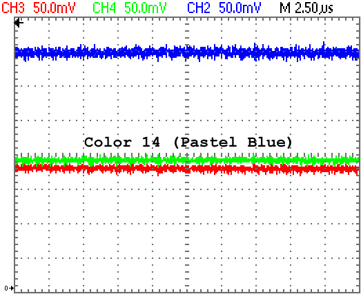
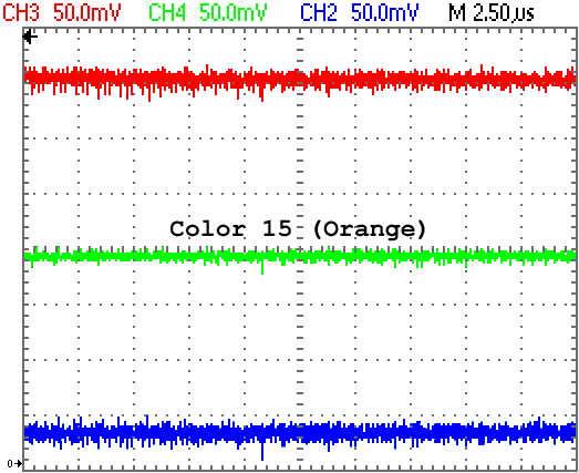
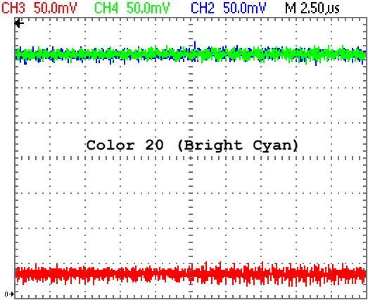
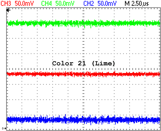
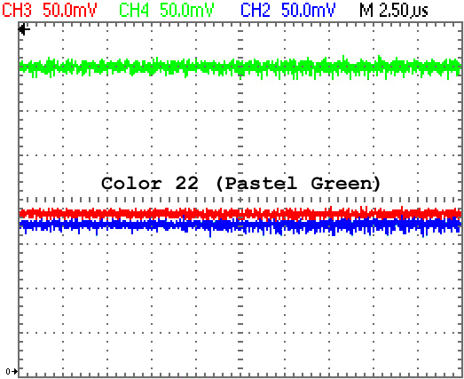
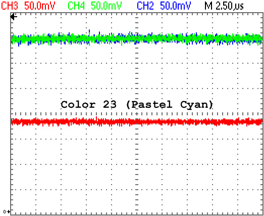
You will also find the real RGB levels as measured on the outputs of a 40010 Gate Array (Amstrad CPC 6128) and ASIC (Amstrad 6128Plus). See Appendix I for more informations.
| Color | BASIC | INKR | ASIC | RGB Gate Array | RGB ASIC | |||||||||
|---|---|---|---|---|---|---|---|---|---|---|---|---|---|---|
| GA - ASIC | hexa | binary | (12bits) | Red | Green | Blue | 24bits | Red | Green | Blue | 24bits | |||
 | 0 | #54 | %01011000 | #000 | 0.0000% | 0.9615% | 0.4808% | #000201 | 0.8230% | 2.8807% | 0.8230% | #020702 | ||
 | 1 | #44 | %01000100 | #006 | 0.0000% | 0.9615% | 41.8269% | #00026B | 2.0576% | 2.4691% | 38.6831% | #050663 | ||
 | 2 | #55 | %01010101 | #00F | 4.8077% | 0.9615% | 95.6731% | #0C02F4 | 2.0576% | 2.8807% | 94.6502% | #0507f1 | ||
 | 3 | #5C | %01011100 | #060 | 42.3077% | 0.9615% | 0.4808% | #6C0201 | 40.3292% | 2.4691% | 0.0000% | #670600 | ||
 | 4 | #58 | %01011000 | #066 | 41.3462% | 0.9615% | 40.8654% | #690268 | 40.7407% | 2.8807% | 39.0947% | #680764 | ||
 | 5 | #5D | %01011101 | #06F | 42.3077% | 0.9615% | 94.7115% | #6C02F2 | 40.7407% | 2.8807% | 94.6502% | #6807F1 | ||
 | 6 | #4C | %01001100 | #0F0 | 95.1923% | 1.9231% | 2.4038% | #F30506 | 99.1770% | 2.8807% | 1.6461% | #FD0704 | ||
 | 7 | #45 | %01000101 | #0F6 | 94.2308% | 0.9615% | 40.8654% | #F00268 | 100% | 2.8807% | 39.0947% | #FF0764 | ||
 | 8 | #4D | %01001101 | #0FF | 95.1923% | 0.9615% | 95.6731% | #F302F4 | 99.1770% | 2.8807% | 95.0617% | #FD07F2 | ||
 | 9 | #56 | %01010110 | #600 | 0.9615% | 47.1154% | 0.4808% | #027801 | 1.6461% | 40.3292% | 1.2346% | #046703 | ||
 | 10 | #46 | %01000110 | #606 | 0.0000% | 47.1154% | 40.8654% | #007868 | 1.6461% | 40.3292% | 39.0947% | #046764 | ||
 | 11 | #57 | %01010111 | #60F | 4.8077% | 48.0769% | 95.6731% | #0C7BF4 | 2.0576% | 40.3292% | 94.6502% | #0567f1 | ||
 | 12 | #5E | %01011110 | #660 | 43.2692% | 48.0769% | 0.4808% | #6E7B01 | 40.7407% | 40.3292% | 1.6461% | #686704 | ||
 | 13 | #40 | %01000000 | #666 | 43.2692% | 49.0385% | 41.8269% | #6E7D6B | 40.7407% | 40.3292% | 39.0947% | #686764 | ||
 | 14 | #5F | %01011111 | #66F | 43.2692% | 48.0769% | 96.6346% | #6E7BF6 | 40.7407% | 40.3292% | 94.6502% | #6867f1 | ||
 | 15 | #4E | %01001110 | #6F0 | 95.1923% | 49.0385% | 5.2885% | #F37D0D | 99.177% | 40.3292% | 1.6461% | #fd6704 | ||
 | 16 | #47 | %01000111 | #6F6 | 95.1923% | 49.0385% | 41.8269% | #F37D6B | 99.177% | 40.3292% | 38.6831% | #fd6763 | ||
 | 17 | #4F | %01001111 | #6FF | 98.0769% | 50% | 97.5962% | #FA80F9 | 99.177% | 40.3292% | 94.6502% | #fd67f1 | ||
 | 18 | #52 | %01010010 | #F00 | 0.9615% | 94.2308% | 0.4808% | #02F001 | 1.6461% | 95.8848% | 0.823% | #04f502 | ||
 | 19 | #42 | %01000010 | #F06 | 0.0000% | 95.1923% | 41.8269% | #00F36B | 1.6461% | 95.8848% | 38.2716% | #04f562 | ||
 | 20 | #53 | %01010011 | #F0F | 5.7692% | 95.1923% | 94.7115% | #0FF3F2 | 1.6461% | 95.8848% | 94.6502% | #04f5f1 | ||
 | 21 | #5A | %01011010 | #F60 | 44.2308% | 96.1538% | 1.4423% | #71F504 | 40.7407% | 95.8848% | 0.0000% | #68f500 | ||
 | 22 | #59 | %01011001 | #F66 | 44.2308% | 95.1923% | 41.8269% | #71F36B | 40.7407% | 95.8848% | 39.0947% | #68f564 | ||
 | 23 | #5B | %01011011 | #F6F | 44.2308% | 95.1923% | 95.6731% | #71F3F4 | 40.7407% | 95.8848% | 94.6502% | #68f5f1 | ||
 | 24 | #4A | %01001010 | #FF0 | 95.1923% | 95.1923% | 5.2885% | #F3F30D | 99.5885% | 95.8848% | 1.6461% | #fef504 | ||
 | 25 | #43 | %01000011 | #FF6 | 95.1923% | 95.1923% | 42.7885% | #F3F36D | 99.177% | 95.8848% | 38.6831% | #fdf563 | ||
 | 26 | #4B | %01001011 | #FFF | 100% | 95.1923% | 97.5962% | #FFF3F9 | 99.177% | 95.8848% | 94.2387% | #fdf5f0 | ||
 | 27⇒13 | #41 | %01000001 | #666 | 43.2692% | 48.0769% | 42.7885% | #6E7B6D | 39.9177% | 39.9177% | 38.2716% | #666662 | ||
 | 28⇒7 | #48 | %01001000 | #0F6 | 95.1923% | 0.9615% | 40.8654% | #F30268 | 98.3539% | 2.0576% | 38.2716% | #fb0562 | ||
 | 29⇒25 | #49 | %01001001 | #FF6 | 95.1923% | 95.1923% | 41.8269% | #F3F36B | 98.3539% | 95.4733% | 37.8601% | #fbf361 | ||
 | 30⇒1 | #50 | %01010000 | #006 | 0% | 0.9615% | 40.8654% | #000268 | 1.2346% | 1.6461% | 37.037% | #03045e | ||
 | 31⇒19 | #51 | %01010001 | #F06 | 0.9615% | 95.1923% | 41.8269% | #02F36B | 1.2346% | 95.4733% | 37.8601% | #03f361 | ||
INKR on the Plus range
When you execute an INKR command on the Amstrad Plus, the ASIC will automagically convert the 5bits color-code to it's corresponding 12bits RGB value and update it's appropriate color register (which are all available in the ASIC I/O page).
There is also a slight color difference between ASIC machines and those with a real Gate Array. The Red, Green and Blue levels produced for each of the 32 color-codes between the CPC and the Plus are close, but not equals. This won't be a problem most of the time but as soon as you start combining differents colors together (dithering and mostly flippping), the differences are accumulating and can be much more annoying (ask SuperSylvestre about that if you dare :).
INKR timings
The effect of an INKR command appears almost immediatly always with the same timings, but the change is not in sync with the character display of the CRTC so the new color appears somehow in the middle of a character (the CRTC display unit).
The tables below show the pixels in a CRTC character and when the effect of an INKR command appears (the blue cells).
Amstrad CPC (real Gate Array)
With a real Gate Array, the INKR effect appears in the middle of a CRTC character. But there's a slight timing difference in the video RAM rasterization between the early Gate Array versions (40007 and 40008) and the last one (40010) produced by Amstrad.
Gate Array 40010
The 40010 version of the Gate Array was initially released with the CPC 6128 and also used in the latest series of CPC 464 and 664 produced by Amstrad. So you might find it in pretty much any CPC models.
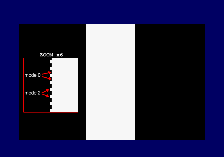
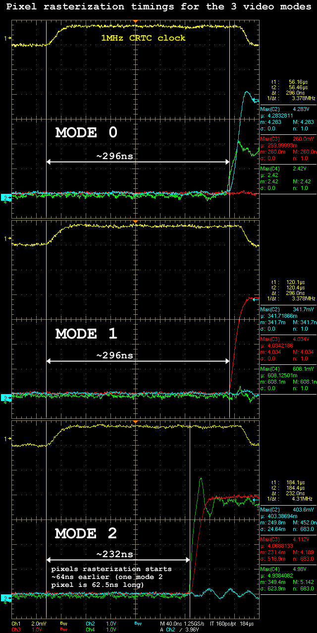
When in video mode 2 (640x200x2c), the 40010 starts rasterizing the video-ram exactly one mode 2 pixel earlier than in the mode 1 and 0, therefore the graphics are shifted to the left by one pixel mode 2 (see Appendix II). But since the INKR timing remains the same, it's effect seems to appear one pixel too late.
| video mode | Pixels in a CRTC character | ||||||||||||||||
|---|---|---|---|---|---|---|---|---|---|---|---|---|---|---|---|---|---|
| 0 | 1 | 2 | 3 | 4 | |||||||||||||
| 1 | 1 | 2 | 3 | 4 | 5 | 6 | 7 | 8 | |||||||||
| 2 | 2 | 3 | 4 | 5 | 6 | 7 | 8 | 9 | 10 | 11 | 12 | 13 | 14 | 15 | 16 | 1 | |
| 3 | 1 | 2 | 3 | 4 | |||||||||||||
Gate Array 40007, 40008 and costdown
On these two versions, the rasterization always starts at the same time, no matter what the video mode is.
| video mode | Pixels in a CRTC character | ||||||||||||||||
|---|---|---|---|---|---|---|---|---|---|---|---|---|---|---|---|---|---|
| 0 | 1 | 2 | 3 | 4 | |||||||||||||
| 1 | 1 | 2 | 3 | 4 | 5 | 6 | 7 | 8 | |||||||||
| 2 | 1 | 2 | 3 | 4 | 5 | 6 | 7 | 8 | 9 | 10 | 11 | 12 | 13 | 14 | 15 | 16 | |
| 3 | 1 | 2 | 3 | 4 | |||||||||||||
Amstrad Plus (ASIC)
| video mode | Pixels in a CRTC character | ||||||||||||||||
|---|---|---|---|---|---|---|---|---|---|---|---|---|---|---|---|---|---|
| 0 | 1 | 2 | 3 | 4 | |||||||||||||
| 1 | 1 | 2 | 3 | 4 | 5 | 6 | 7 | 8 | |||||||||
| 2 | 1 | 2 | 3 | 4 | 5 | 6 | 7 | 8 | 9 | 10 | 11 | 12 | 13 | 14 | 15 | 1 | |
| 3 | 1 | 2 | 3 | 4 | |||||||||||||
The INKR effect on a Plus appears at 1/4 of a CRTC character in any video modes.
As you can see, the effect of an INKR command doesn't appear at the same time on a Plus than on a CPC. If you intend to do some split-raster aligned with graphics at pixel precision and that should run on both CPC and Plus machines, you may have to hack arround the ASIC soft-scroll register (SSR) on the Plus to scroll the graphics and compensate the Plus timings to match those on the CPC (but it might not be easy in some case…).
RGB to BASIC color code
To calculate the BASIC color-code from RGB levels (off, half, full), you can use something like this (pseudocode) :
; R,G and B corresponding to the BASIC color 5
R=50%
G=0%
B=100%

; Initialize our 5bits color code to zero (black)
ink=0

; Process the Red
if(R==100%) {
	ink=ink+6
} else if(R==50%) {
	ink=ink+3
}

; Process the Green
if(G==100%) {
	ink=ink+18
} else if(R==50%) {
	ink=ink+9
}

; Process the Blue
if(B==100%) {
	ink=ink+2
} else if(R==50%) {
	ink=ink+1
}

; and that's it, variable ink now hold 5.
RMR
This register control the interrupt counter (reset), the upper and lower ROM paging and the video mode.
| RMR | Commands | ||||||
|---|---|---|---|---|---|---|---|
| 7 | 6 | 5 | 4 | 3 | 2 | 1 | 0 |
| 1 | 0 | 0 | I | UR | LR | VM | |
- I : if set (1), this will reset the interrupt counter.
- UR : Enable (0) or Disable (1) the upper ROM paging (&C000 to &FFFF). You can select which upper ROM with the I/O address &DF00.
- LR : Enable (0) or Disable (1) the lower ROM paging.
- VM : Select the video mode 0,1,2 or 3 (it will take effect after the next HSync).
Video Mode
There's 4 differents video mode available. Mode 0,1 and 2 are the most widely known and are available from BASIC (with the MODE n instruction). Mode 3 is a bit weird but may be useful in some very special cases.
You can change the mode with RMR bits 0,1 (VM). It will take effect after the next HSync is issued.
| Byte/Pixel structure | ||||||||||||||||||||
|---|---|---|---|---|---|---|---|---|---|---|---|---|---|---|---|---|---|---|---|---|
| VM (Mode) | 7 | 6 | 5 | 4 | 3 | 2 | 1 | 0 | On screen display | Details | ||||||||||
| %00 (0) | A0 | B0 | A2 | B2 | A1 | B1 | A3 | B3 | A | B | 4bits/pixels (16 colors), 2 pixels/byte (160×200) | |||||||||
| %01 (1) | A0 | B0 | C0 | D0 | A1 | B1 | C1 | D1 | A | B | C | D | 2bits/pixels (4 colors), 4 pixels/byte (320×200) | |||||||
| %10 (2) | A | B | C | D | E | F | G | H | A | B | C | D | E | F | G | H | 1bit/pixel (2 colors), 8 pixels/byte (640×200) | |||
| %11 (3) | A0 | B0 | x | x | A1 | B1 | x | x | A | B | 2bits/pixels (4 colors), 2 pixels/byte (160×200) | |||||||||
To have a look at these differents video mode in action, you can check my CPC graphics archive.
Note that the Gate Array needs an HSync of at least 2μs to update it's internal byte⇒pixels decoder with a new video mode. The HSync duration is defined by the CRTC Register 3 and is usually set to 14µs.
Exemple
; The usual RMR command to select video mode 0 (bit 1,0=%00)
ld bc,&7F8C
out (c),c
; This will also disable Upper ROM (bit3=%1) and Lower Rom (bit2=%1) paging,
; you should avoid doing that when the firmware is up and running (there's a
; firmware vector to select video mode).
VRAM display timings
On a real Gate Array 40010, when the video mode is set to 2 (640x200x2c), the display will start one pixel (mode 2) earlier than in the others video modes (0,1 and 3), thus shifting the scanlines 1 pixel mode 2 to the left. See INKR timings and Appendix II for more details.
The video RAM rasterization timings on a 40007 Gate Array and ASIC are not affected by the video mode. I haven't verified the 40008 version yet.
Upper ROM
The RMR Bit3 (UR) is used to page the Upper ROM from #C000 to #FFFF in the CPU address space.
| UR | #0000-#3FFF | #4000-#7FFF | #8000-#BFFF | #C000-#FFFF | |
|---|---|---|---|---|---|
| 0 | unaffected | Upper ROM | |||
| 1 | unaffected | ||||
When the Upper ROM is enabled:
- all CPU read operations between #C000 to #FFFF will read the ROM.
- all CPU write operations between #C000 to #FFFF will affect the “underlying” RAM (depending on the MMR configuration).
You can select which Upper ROM is paged with the Upper ROM register at the I/O address &DF00. But, this register doesn't work exactly the same on the CPC and Plus :
Amstrad CPC
On the CPC, it's simple, you can select any logical ROM id from 0 to 255 and that's it:
ld bc,&DF00 ; C=0 => ROM 0 is the BASIC
out (c),c   ; select ROM 0 as the active Upper ROM

ld bc,&7F00+%10000110 ; change the RMR register to enable the Upper ROM paging (bit3=0)
out (c),c             ; (note that we are forced to affect the video mode too, bit 1,0)

; from now on, the BASIC ROM is paged from #C000 to #FFFF

; You can change the Upper ROM at anytime
ld bc,&DF07 ; C=7 => ROM 7 is the AmsDOS on a 664/6128 or 464 with a DDI
out (c),c

; from now on, the AMSDOS ROM is paged from #C000 to #FFFF

; And now we disable the Upper ROM paging
ld bc,&7F00+%10001110 ; bit3=1
out (c),c
The built-in Upper ROMs in a CPC are :
- 0 - BASIC
- 7 - AmsDOS (664, 6128 or 464 with DDI)
Amstrad Plus
The Plus has two ROMs systems:
- ROMs on a Romboard (or similar device) are assigned with a logical ROM id, from 0 to 127.
- ROMs on a cartdridge are assigned with a physical ROM id, from 0 to 31.
The ROM ID sent to the Upper ROM register at the I/O address &DF00 should be coded as shown in the table below:
| 7 | 6 | 5 | 4 | 3 | 2 | 1 | 0 | Description |
|---|---|---|---|---|---|---|---|---|
| 0 | L | L is a logical ROM ID from 0 to 127 | ||||||
| 1 | x | x | P | P is a physical ROM ID on the cartdridge from 0 to 31 | ||||
Physical ROM IDs with the green Burnin'Rubber cartdridge shipped with the Plus are :
- 0 : Firmware
- 1 : BASIC
- 2 : unused
- 3 : AmsDOS
- 4 : Burnin'rubber ROM 1/4
- 5 : Burnin'rubber ROM 2/4
- 6 : Burnin'rubber ROM 3/4
- 7 : Burnin'rubber ROM 4/4
A cartdridge can hold a maximum of 32 ROMs (512Kb, without hardware hacking on the cartdridge), with physical IDs from 0 to 31. Unlike the CPC, there's no ROMs built-in the Plus, it has all its system ROMs on the cartdridge, which is problem since the Firmware is designed to deal only with logical ROM IDs!
That's why some of the ROMs on the cartdridge are also assigned with a logical ROM ID, to maintain compatibility:
- Physical ROM 1 (BASIC) on the cartdridge is assigned to the logical ROM 0 too.
- Physical ROM 3 (AmsDOS) on the cartdridge is assigned to the logical ROM 7 too.
This way, the Firmware, BASIC and AmsDOS keep working on a Plus just like they did on a CPC, with logical ROM IDs. But there's something neat with this system: If you have a romboard on your Plus, you can setup a logical ROM 7 with ParaDOS (or whatever) and this will automagically override/disable the AmsDOS from the cartdridge! No hardware modifications are required like on the CPC. The AmsDOS remains accessible trough it's physical ROM ID but is no more assigned to the logical ROM 7.
Lower ROM
The RMR Bit2 (LR) control the lower ROM paging ON(0)/OFF(1).
Amstrad CPC
On a CPC, there's only one Lower ROM : the Amstrad Firmware. And it can only be paged in the lower 16Kb RAM space : #0000 to #3FFF (hence the name, Lower ROM :).
| LR | #0000-#3FFF | #4000-#7FFF | #8000-#BFFF | #C000-#FFFF | ||
|---|---|---|---|---|---|---|
| 0 | Firmware ROM | unaffected | ||||
| 1 | unaffected | |||||
Amstrad Plus
On a Plus, it's getting a little bit more complicated. This bit still controls the Lower ROM paging ON(0)/OFF(1), but you can also use the RMR2 register (only when the ASIC is unlocked) to configure which ROM from the cartdridge (you're no more limited to the only Firmware ROM) must be paged and where (you're not limited to the #0000 to #3FFF like the CPC).
The default setting of the RMR2 register is configured to page the Firmware ROM on the cartdridge from #0000 to #3FFF, just like a CPC would do, to maintain software compatibility.
In all cases, when the Lower ROM is enabled:
- all CPU read operations where the ROM is paged will, fortunatly, read the ROM.
- all CPU write operations where the ROM is paged will affect the “underlying” RAM (depending on the current MMR configuration).
RMR2
The RMR2 register extends the functionnalities of the RMR register about the Lower ROM mapping and also controls the ASIC I/O page mapping (between #4000 to #7FFF) as shown in the table below:
| RMR2 | LRM | ROM ID | ASIC/ROM Mapping | |||||||||||
|---|---|---|---|---|---|---|---|---|---|---|---|---|---|---|
| 7 | 6 | 5 | 4 | 3 | 2 | 1 | 0 | #0000-#3FFF | #4000-#7FFF | #8000-#BFFF | #C000-#FFFF | |||
| 1 | 0 | 1 | 0 | 0 | P | ROM P | ||||||||
| 1 | 0 | 1 | 0 | 1 | P | ROM P | ||||||||
| 1 | 0 | 1 | 1 | 0 | P | ROM P | ||||||||
| 1 | 0 | 1 | 1 | 1 | P | ROM P | ASIC I/O | |||||||
Exemple
; Enable the ASIC I/O page on &4000/&7FFF
; Select &0000/&3FFF as mapping area for the Lower ROM
ld bc,&7FB8 ; %101 11 000
out (c),c
; Disable the ASIC I/O page
; Select &0000/&3FFF as mapping area for the Lower ROM
ld bc,&7FA0 ; %101 00 000
out (c),c
Notes
- The physical ROM P is actually mapped in the CPU address space only if the RMR.LR bit is clear (0 ⇒ mapping ON). So you can use RMR.LR=%1 and RMR2.LRM=%11 to enable only the ASIC I/O page mapping without any Lower ROM mapped anywhere.
- You can only map the first 8 physical ROMs of the cartdridge as Lower ROM. To access physical ROM above 7, you have to use the Upper ROM mapping.
MMR
The MMR register is provided by the extended RAM expansion. On a 128Kb machine (ie. CPC6128) it is provided by the PAL chip. This register controls how the extended RAM is banked into the CPU address space.
RAM on the Amstrad
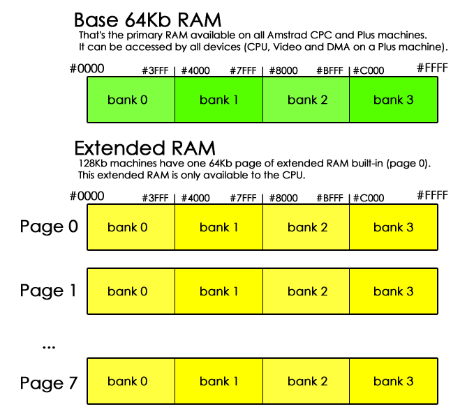 There's basically two types of RAM, the base 64Kb RAM and the extended RAM.
The base 64Kb RAM is the primary RAM available on all Amstrad CPC and Plus models. Beside the CPU, it can be used by other devices (CRTC & Gate Array for the video, DMA channels on the Plus machines). If you're familiar with the Amiga, it's like the chipram.
The extended RAM is provided either by the built-in PAL of 128K models or by some additionnal RAM expansion device connected to the Amstrad. This extended RAM is usually divided into 64Kb pages, each page is made of four 16Kb banks. The regular RMR register supports up to 8 pages, thus 512Kb of extended RAM. Regular? RAM expansions with more than 512Kb usually provide one, or more, custom RMR registers (located at differents I/O addresses, usually &7E00, &7D00, etc). One for each 512Kb block of additionnal memory. The extended RAM is only available to the CPU.
Regular RMR Register
The table below shows the differents memory mapping configurations supported by the RMR register provided by the PAL on 128K machines.
| MMR | 64K page | S | MM | CPU Memory Mapping | |||||||||||
|---|---|---|---|---|---|---|---|---|---|---|---|---|---|---|---|
| 7 | 6 | 5 | 4 | 3 | 2 | 1 | 0 | #0000-#3FFF | #4000-#7FFF | #8000-#BFFF | #C000-#FFFF | ||||
| 1 | 1 | x | 0 | 0 | 0 | Bank 0:Base 64Kb | Bank 1:Base 64Kb | Bank 2:Base 64Kb | Bank 3:Base 64Kb | ||||||
| 1 | 1 | p | 0 | 0 | 1 | Bank 0:Base 64Kb | Bank 1:Base 64Kb | Bank 2:Base 64Kb | Bank 3:Page p | ||||||
| 1 | 1 | p | 0 | 1 | 0 | Bank 0:Page p | Bank 1:Page p | Bank 2:Page p | Bank 3:Page p | ||||||
| 1 | 1 | p | 0 | 1 | 1 | Bank 0:Base 64Kb | Bank 3:Base 64Kb | Bank 2:Base 64Kb | Bank 3:Page p | ||||||
| 1 | 1 | p | 1 | b | Bank 0:Base 64Kb | Bank b:Page p | Bank 2:Base 64Kb | Bank 3:Base 64Kb | |||||||
Programming exemples
Accessing the extended 64Kb RAM on a 6128 :
; &C4=%11 000 1 00  => bank 0 of page 0 is paged to &4000/&7FFF
ld bc,&7FC4
out (c),c

; now all RAM Read/Write operations done by the CPU between &4000/&7FFF
; will access the bank 0/page 0 of the extended RAM.

; &C0=%11 000 0 00 => restore the base 64Kb RAM linear mapping.
ld bc,&7FC0
out (c),c
Memory mapping in the CPU address space
 Each 16Kb blocks of the 64Kb CPU address space (&0000 to &FFFF) are configurable (with the RMR, RMR2, MMR and URR registers) and can be mapped with differents type of memories: ROM, RAM or the ASIC I/O page on the Plus.
All other devices doing RAM access (eg. Gate Array, ASIC DMAs) are unaffected by this mapping and always use the base 64Kb RAM of the CPC/Plus (the Gate Array read 2 bytes from the base 64Kb RAM every microseconds to generate the RGB video signals. The 3 ASIC-DMAs also read 2 bytes each from the base 64Kb RAM while the HSync is active).
Because it is possible to map differents memory types in the same CPU address space at the same time, each memory type have a priority. When the CPU is reading from or writing to an address, only the memory type with the highest priority will respond to the CPU.
| CPU access | ||
|---|---|---|
| Priority | CPU Read | CPU Write |
| 1 | ROM | |
| 2 | ASIC I/O | |
| 3 | Extra RAM banks | |
| 4 | Base 64Kb RAM | |
Pinout
40008, 40010
The 40008 is an improved version of the 40007 and came up with the CPC 664. The 40010 is again an improved version and came up with the CPC 6128. Both versions are pinout compatible.
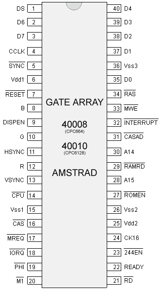
| Pinout | In/Out | Name | Description |
|---|---|---|---|
| 4 | OUT | CCLK | |
| 5 | OUT | SYNC | |
| 6 | IN | VDD1 | |
| 7 | IN | RESET | |
| 8 | OUT | BLUE | |
| 9 | IN | DISPEN | |
| 10 | OUT | GREEN | |
| 11 | IN | HSYNC | |
| 12 | OUT | RED | |
| 13 | IN | VSYNC | |
| 14 | OUT | /CPU | |
| 15 | IN | VSS1 | |
| 16 | OUT | /CAS | |
| 17 | IN | /MERQ | |
| 18 | IN | /IORQ | |
| 19 | OUT | /PHI | |
| 20 | IN | /M1 | |
| 21 | IN | /RD | |
| 22 | OUT | READY | |
| 23 | OUT | /244EN | |
| 24 | IN | CK16 | |
| 25 | IN | VDD2 | |
| 26 | IN | VSS2 | |
| 27 | OUT | /ROMEN | |
| 28 | IN | A15 | |
| 29 | OUT | /RAMRD | |
| 30 | IN | A14 | |
| 31 | OUT | /CASAD | |
| 32 | OUT | /INTERRUPT | |
| 33 | OUT | /MWE | |
| 34 | OUT | /RAS | |
| 35 | IN/OUT | D0 | |
| 36 | IN | VSS3 | |
| 37 | IN/OUT | D1 | |
| 38 | IN/OUT | D2 | |
| 39 | IN/OUT | D3 | |
| 40 | IN/OUT | D4 | |
| 1 | IN/OUT | D5 | |
| 2 | IN/OUT | D6 | |
| 3 | IN/OUT | D7 |
40007
The 40007 Gate Array is the one built-in the firsts CPC 464. It is not pinout compatible with the later one (40008 and 40010). Note that the last CPC 464 produced by Amstrad were fitted with a 40008 since the quality of the original 40007 was not very good.
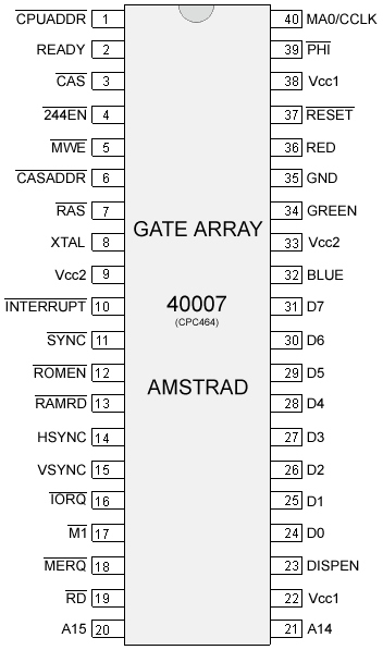
| Pinout | In/Out | Name | Description |
|---|---|---|---|
| 1 | OUT | /CPUADDR | Control Process Unit ADDress. 1MHz clock signal for the AY3 and indicate which of the CPU or Gate Array have access to the RAM. |
| 2 | OUT | READY | |
| 3 | OUT | /CAS | Column Address |
| 4 | OUT | /244EN | 244 Enable |
| 5 | OUT | /MWE | Memory Write Enable |
| 6 | OUT | /CASADDR | CAS Address |
| 7 | OUT | /RAS | Row Address |
| 8 | IN | XTAL | 16MHz clock |
| 9 | IN | VCC2 | 5 volts |
| 10 | OUT | /INTERRUPT | 3.3ms active low pulse to trigger a maskable interrupt on the CPU |
| 11 | OUT | /SYNC | SYNCHronization (video) |
| 12 | OUT | /ROMEN | ROM ENable |
| 13 | OUT | /RAMRD | RAM ReaD |
| 14 | IN | HSYNC | Horizontal SYNCHronization (CRTC) |
| 15 | IN | VSYNC | Vertical SYNCHronization (CRTC) |
| 16 | IN | /IORQ | Input/Output ReQuest (CPU) |
| 17 | IN | /M1 | Pulse signal which indicate the CPU issued an INT request (CPU) |
| 18 | IN | /MERQ | MEmory ReQuest (CPU) |
| 19 | IN | /RD | ReaD (CPU) |
| 20 | IN | A15 | Used for the I/O port address decoding |
| 21 | IN | A14 | Used for the I/O port address decoding |
| 22 | IN | Vcc1 | 5 volts |
| 23 | IN | DISPEN | DISPlay ENable (CRTC) |
| 24 | IN/OUT | D0 | DATA Bit |
| 25 | IN/OUT | D1 | DATA Bit |
| 26 | IN/OUT | D2 | DATA Bit |
| 27 | IN/OUT | D3 | DATA Bit |
| 28 | IN/OUT | D4 | DATA Bit |
| 29 | IN/OUT | D5 | DATA Bit |
| 30 | IN/OUT | D6 | DATA Bit |
| 31 | IN/OUT | D7 | DATA Bit |
| 32 | OUT | BLUE | |
| 33 | IN | Vcc2 | 5 volts |
| 34 | OUT | GREEN | |
| 35 | IN | GND | GrouND |
| 36 | OUT | RED | |
| 37 | IN | /RESET | |
| 38 | IN | Vcc1 | 5 volts |
| 39 | OUT | /PHI | 4MHz CPU clock |
| 40 | OUT | MA0/CCLK | 1MHz RAM refresh clock |
The Gate Array Simulator
- source: CPC-Wiki
The Gate Array was the only component of the Amstrad CPC, which was not a standard one but developed by Amstrad. Before it could be produced as a single chip, they had to make tests with a prototype, which was a single print on top of the actual motherboard.
Appendix
I: RGB outputs
Gate Array on the Amstrad CPC
|
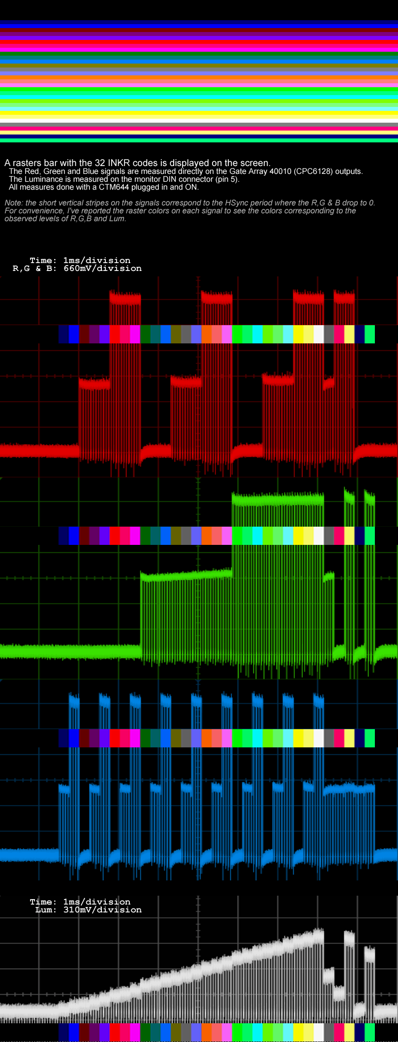
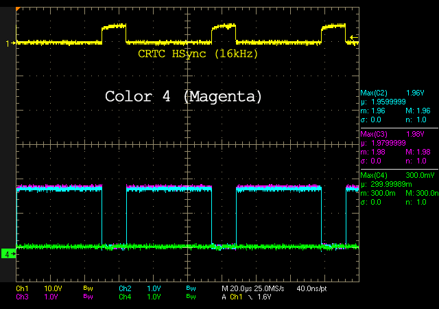
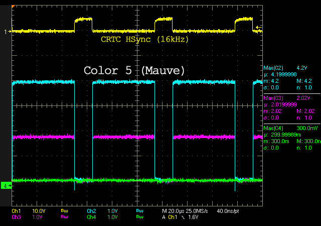
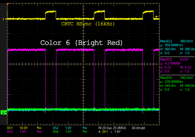
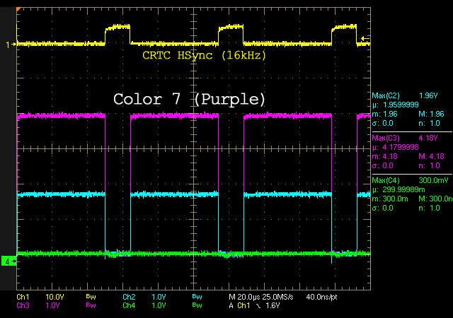
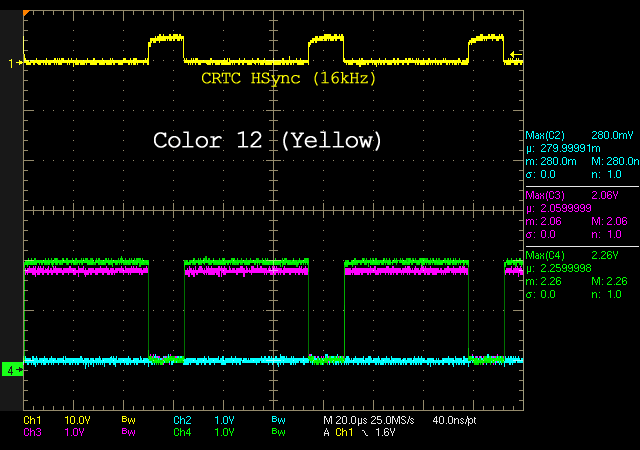
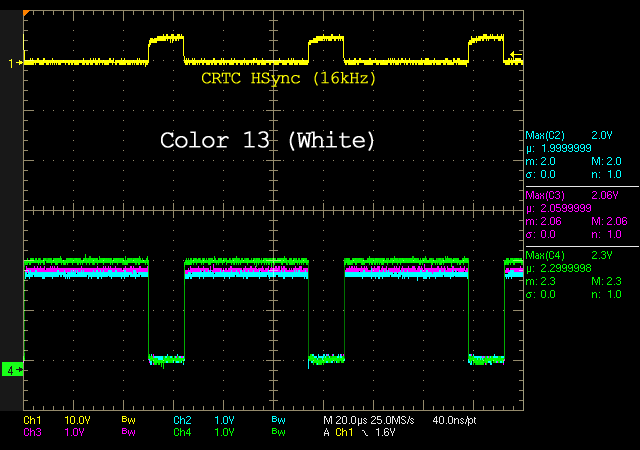
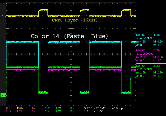
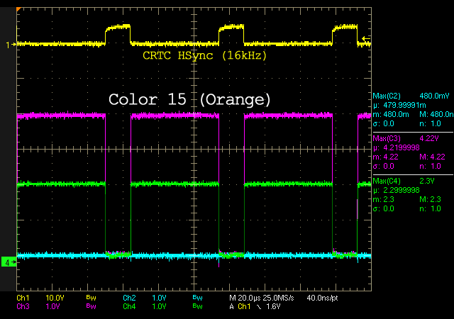
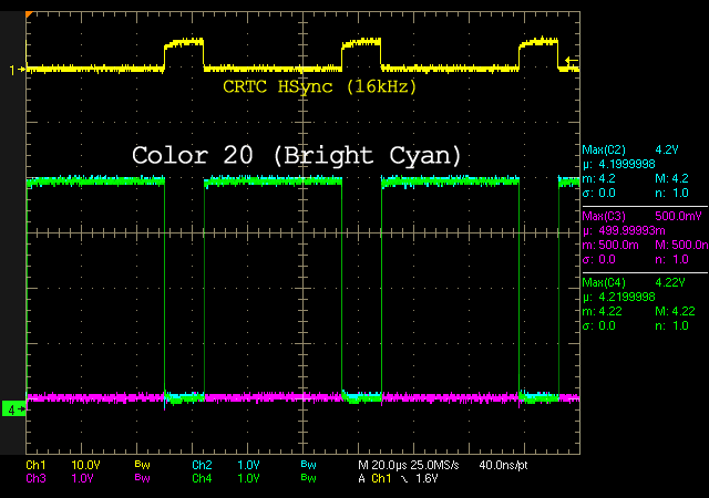
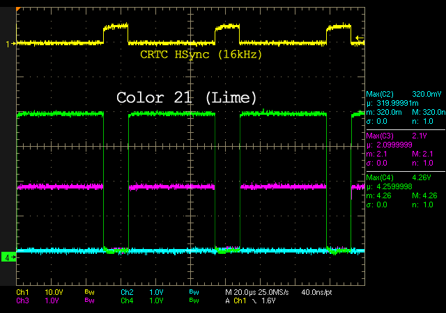
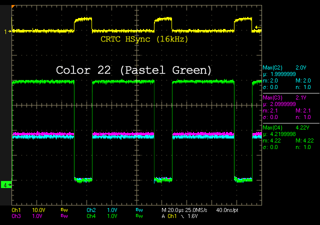
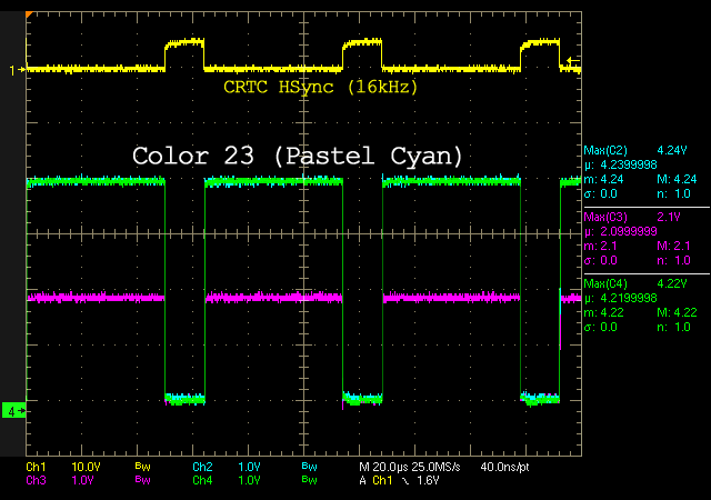
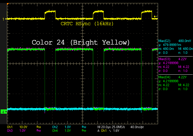
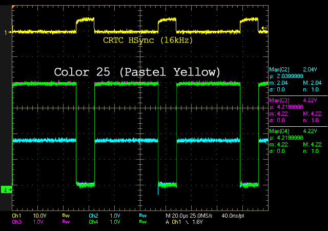
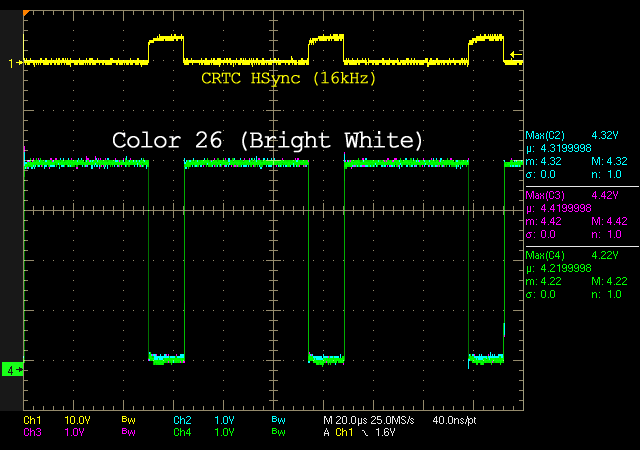
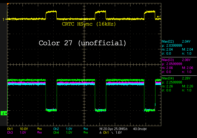
If you take a close look at the RGB outputs of the Gate Array (on a real Amstrad CPC), you should notice that there's really strange things happening there… Half intensityThe Gate Array is known to work with a 3 states logic to produce the R,G and B signals:
So we get 3x3x3=27 colors from this. Clean and simple eh? First, that half-intensity is clearly not that half at all (look at the RGB values in the INKR table above and try to catch a 50% if you can :) and each of the Red, Green and Blue signals also have their own half intensity levels! And the Green half intensity level is significantly greater than the Red and Blue half intensity. Moreover, if you look at the half intensity on all the colors range, from color 0 (black) to 26 (white), you will notice that the closer you get from color 26 (white), the half intensity levels are all slowly increasing. LuminanceIdeally, the luminance should be a nice wave ramp. But since the green half intensity level is greater than the two others, it also affect the luminance by introducing 2 smalls discontinuities in the ramp. MonitorThe monitor also affect the video signals because of it's load impedance. Depending on the monitor, the signals levels will be significantly reduced (all by the same amount fortunately) and their shape will be affected as well (the clean square waves will be smoothed and won't have fast and straight transitions anymore). Moreover, the Gate Array is not isolated or protected from whatever is plugged in the video output connector. Therefore, a faulty monitor could eventually blow up the Gate Array and other electronic parts in the CPC. |
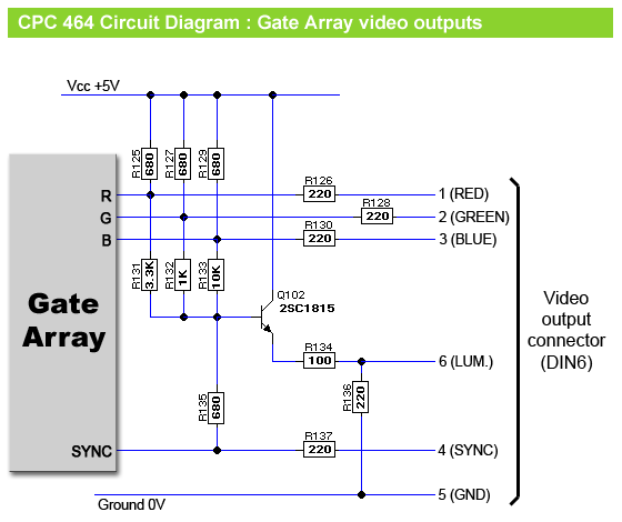
Circuit diagrams: CPC 6128 and 664
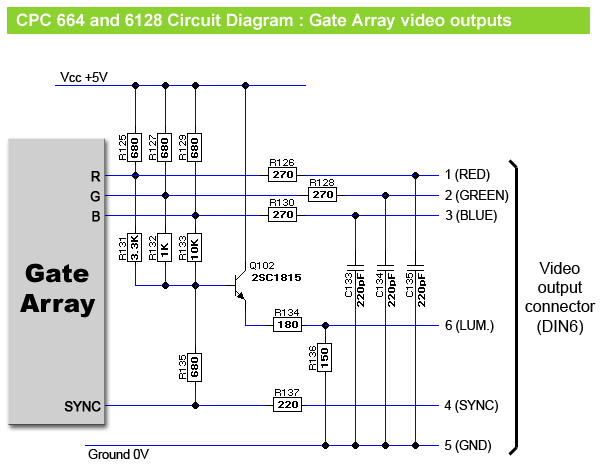 The only differences with the 464 RGB outputs are those 3 capacitors which will filter hifrequency noise on the RGB signals and some differents resistors values (but it doesn't make any significant changes on what you see on the screen).
Circuit diagrams: CPC 464
RGB levels of a 40010 Gate Array
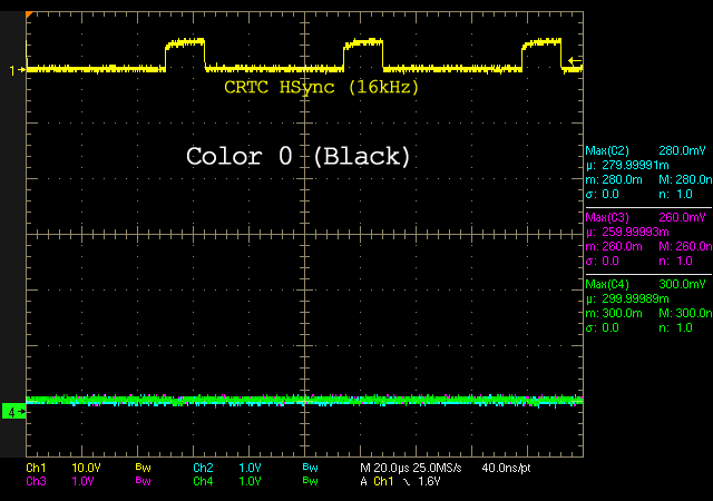
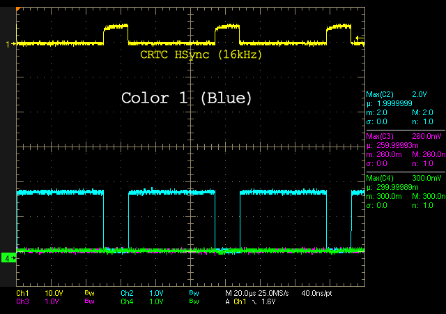
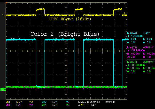
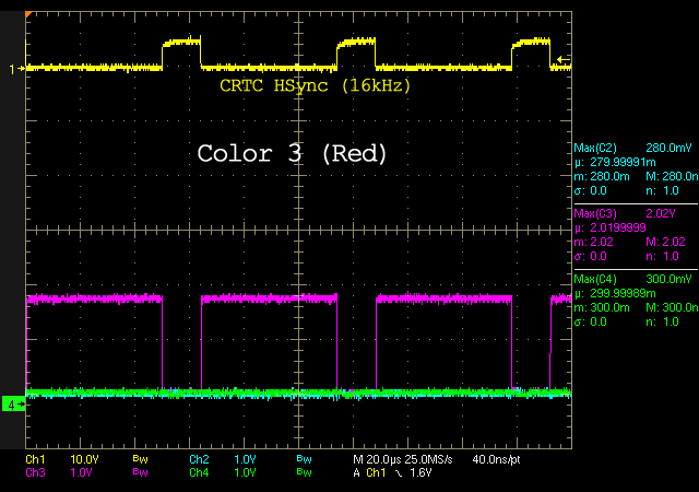
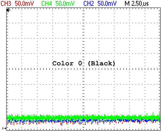
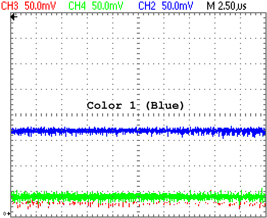
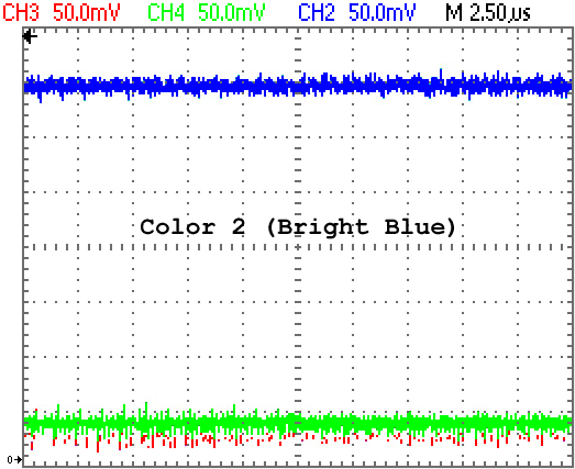
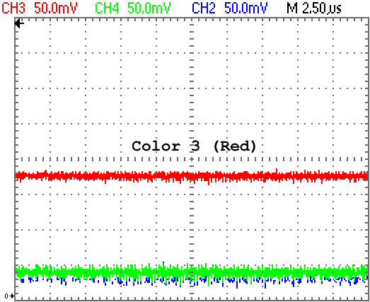
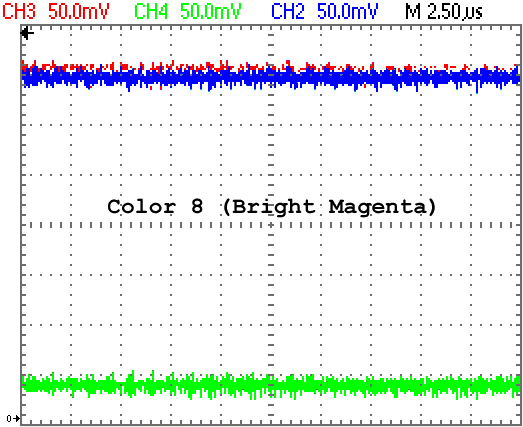
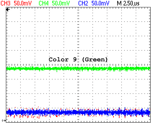
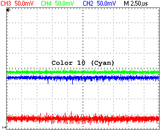
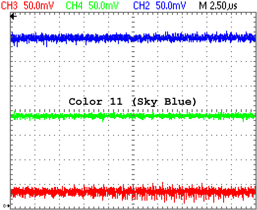
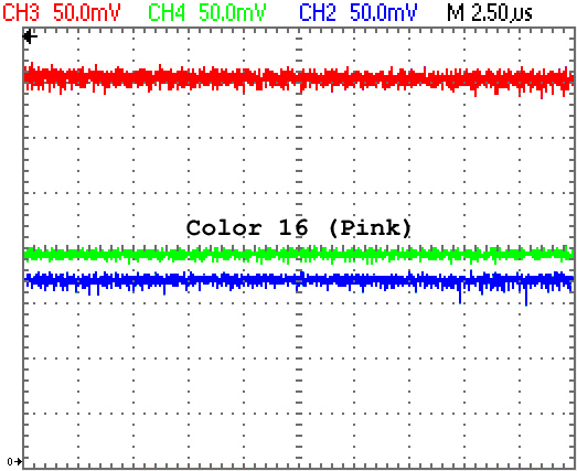
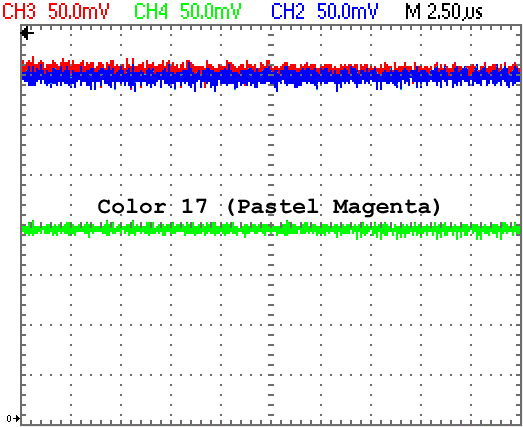
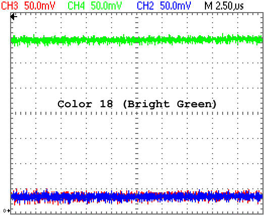
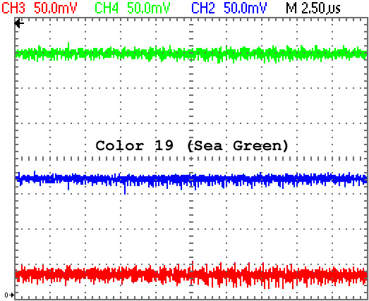
RGB signals measured directly on the outputs (pins 8,10 & 12) of a Gate Array 40010 (with a CTM644 plugged in and switched ON).
RGB levels of a 40008 Gate Array
I don't have any CPC with a 40008.
RGB levels of a 40007 Gate Array
RGB signals measured directly on the outputs (pins 32, 34 & 36) of a Gate Array 40007 (with a CTM644 plugged in and switched ON).
RGB levels of a Costdown Gate Array
I don't have any costdown CPC.
3x4bits DAC on the Amstrad Plus
Measurement is planned, come back later again :)
II: VRAM Rasterization timings
|
(todo) Tested:
Todo:
Test programJust type this little BASIC program and RUN it (or download it as DSK file): 10 MODE 2:INK 0,0:PAPER 15:WINDOW 30,50,1,25:CLS 20 FOR i=1 TO 15:INK i,26:NEXT 30 RESTORE 40:FOR i=0 TO 21:READ d:POKE &8000+i,d:NEXT:CALL &8000 40 DATA &F3,&01,&8E,&7F,&ED,&49,&06,&0E 41 DATA &10,&FE,&01,&8C,&7F,&ED,&49,&06 42 DATA &0D,&10,&FE,&00,&18,&EB The lines of DATA correspond to this tiny assembly routine: org &8000 di ; prevent the firmware interrupt ; to kick in loop ld bc,&7F8E ; switch to video mode 2 out (c),c ld b,14 ; wait to sync with the djnz $ ; HSync period (64us) ld bc,&7F8C ; switch to video mode 0 out (c),c ld b,13 djnz $ nop jr loop ; infinite loop On a 40010 Gate Array, the right and left egdes of the white box wont be straight: |
